You are here
Back to topNegative Voltage Generation in Buck Converter
In the application environment of smart manufacturing, it is often necessary to feedback big data through environmental sensors to make judgments and corrections to the system. In these analog signals such as temperature, humidity, etc., sensor circuits with positive and negative power supply bias are required to do detection to avoid data distortion.
In the design of system power supply, most of them need to use a transformer to generate negative voltage, which makes it inconvenient to use the circuit, so it is not easy to obtain negative voltage. In order to make it easier to obtain the negative voltage, the output terminal of the buck converter is reversely connected and transformed into the characteristics of the buck-boost converter to obtain the output negative voltage.
This article will discuss the reverse connection of the output of a buck converter, what precautions should be taken before it generates a negative output voltage, and analyze the differences in the converter circuit.
1. What is Negative Voltage
The magnitude of the voltage is relative to the selected reference voltage, and the negative voltage in the circuit refers to a lower voltage. When the actual voltage is lower than the reference point, the voltage is negative. The most common reference zero is ground, which is zero volts. Another situation is when the voltage reference direction and the current reference direction are selected to be opposite, the voltage will also be negative.
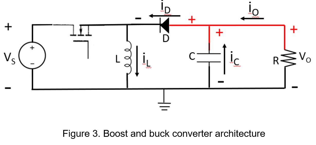
The following will briefly introduce two basic power converter topologies, as shown in Figure 1 and Figure 3, and a process description explaining why the output of a buck converter is reversed.
Figure 1 shows the basic buck converter circuit topology.
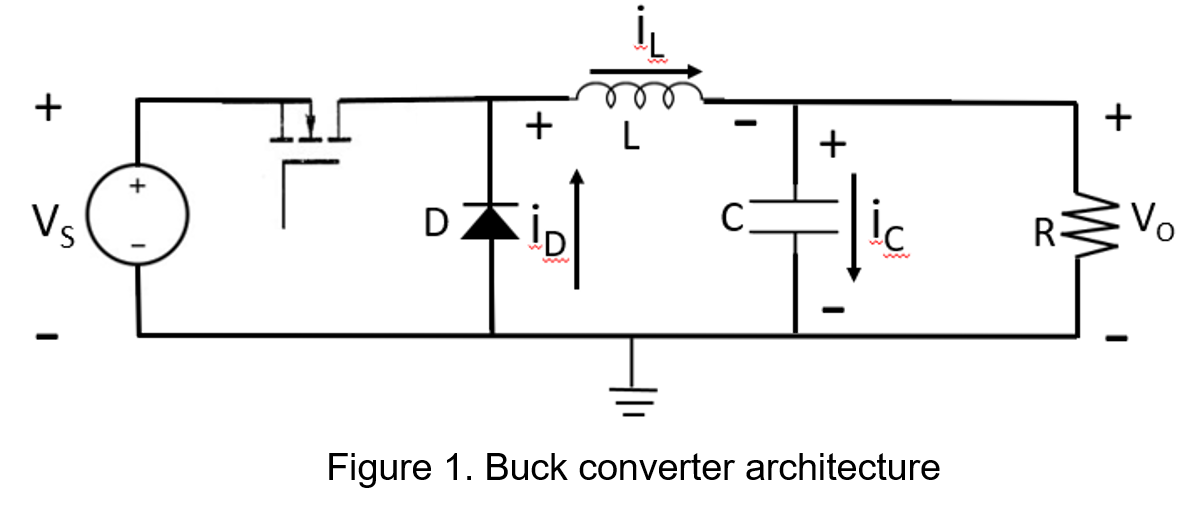
Figure 2 shows the reverse connection of the output of the buck converter. Since the ground is moved to the original position of the positive end of Vo, the circuit structure of the output end is forced to change.
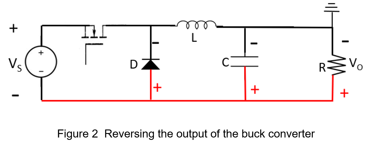
Figure 3 shows the position where the ground is connected back to the negative terminal of VO in Figure 2. After the internal components are changed, the structure is the same as the basic buck-boost converter circuit topology. In addition, since the current flow is different from the preset position, the output voltage opposite polarity.
2. Input Voltage Ripple
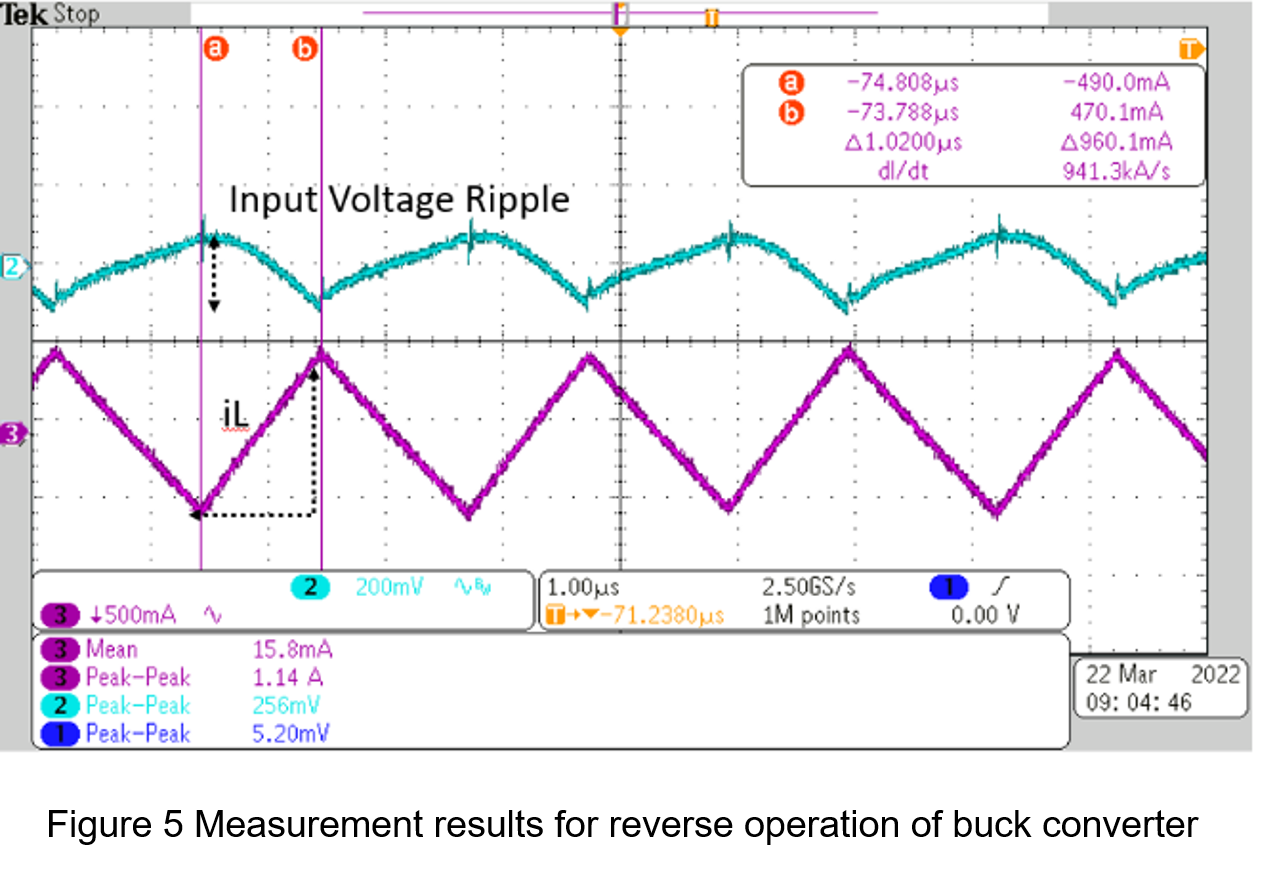
When the output positive and negative terminals of a buck converter are reversely connected, the internal structure of the circuit is forced to change, causing the input filter capacitor to act as a circuit breaker, resulting in two to three times larger input voltage ripple. The following experiment uses a buck converter with an inductance specification of 15uH and a switching frequency of 450kHz.
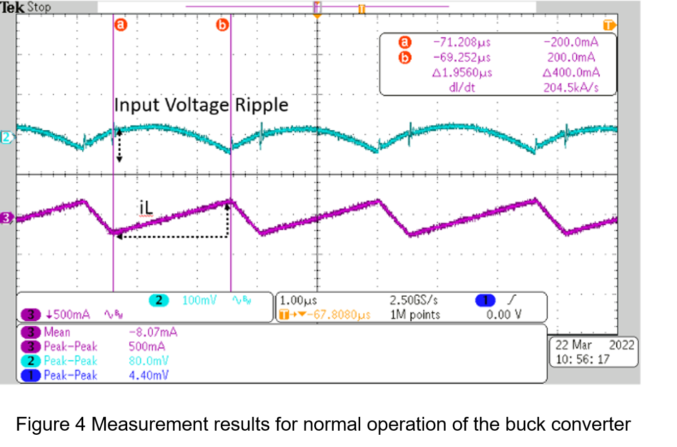
Figure 5 shows the buck converter output with positive and negative reversal and an input voltage of 15V and an output current of 0.3A, where the input peak to peak ripple voltage is 256mV.
3. The Relationship between Output Voltage Range and Inductance
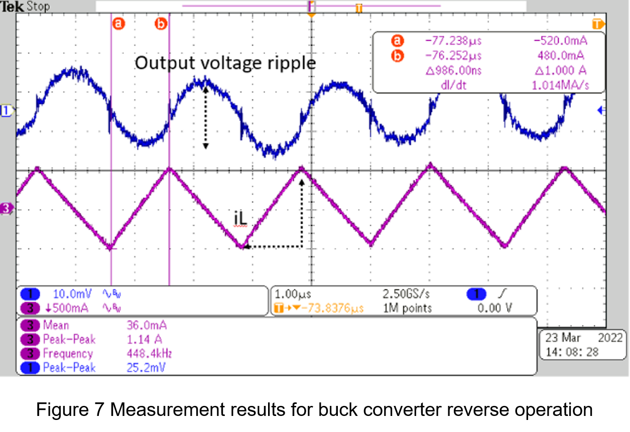
The above-mentioned buck converter has the characteristics of a buck-boost converter when the positive and negative terminals of the output are reversely connected, but due to the different characteristics of the two, it means that the di/dt is different when it is turned on and off. The direct conversion of a buck converter to a buck-boost converter will cause the current flowing through the inductor to be instantaneously higher, resulting in insufficient inductance to provide energy. Therefore, it is recommended to maintain the operation below half of the output load current when the reverse connection is performed, otherwise the circuit will cause resonance. The result causes the inductor current to fluctuate suddenly.
Figure 6 shows the inductor current measurement waveform for normal operation of the buck converter with an input voltage of 15V and an output load current of 0.6A, where di/dt of inductor current is 200KA/s.
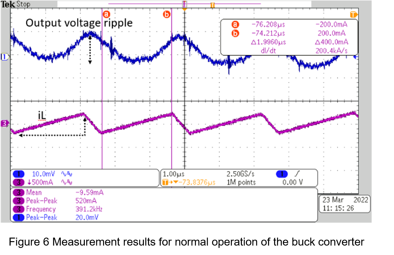
Figure 7 shows the measured inductance current waveform, the di/dt is1.014M A/s for reversal operation. An input voltage of 15V and an output load current of 0.6A.
4. Allowable Withstand Pressure Range
The biggest influence of the difference in withstand voltage is on the input and output voltage of the circuit and the withstand voltage value of the internal components. When a buck converter with an input voltage range of 15 volts to 32 volts and an output voltage of 12 volts, once the output positive and negative terminals are reversely connected, the internal component cross-voltage will increase rapidly and cause permanent damage. In order to avoid this problem, the design will reduce the input voltage range. Generally, the power transistor components of a circuit with a maximum input and output of 32 volts have a withstand voltage of about 35 volts. If the positive and negative terminals of the output are reversely connected and the maximum input voltage is 35 volts, the circuit will burn. Therefore, before starting, you must pay attention to the maximum input voltage range after the output is reversed.
For example, if the maximum input voltage is 32 volts and the maximum output voltage is 12 volts, the maximum input voltage after reversing the positive and negative outputs is only 20 volts. The following is a measurement of the input voltage waveform for normal operation of the buck converter and the withstand voltage of the switch when reversal condition.
Figure 8 shows the VDS withstanding voltage of the power transistor at 33.6V for normal operation of the buck converter and input voltage of 32V.
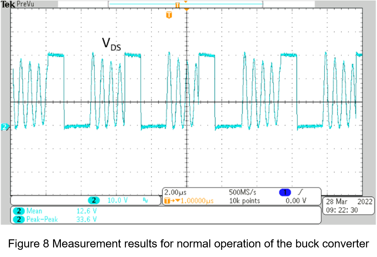
Figure 9 shows the VDS withstanding voltage of the power transistor at 36V for reversal operation of buck converter and 20V input voltage.
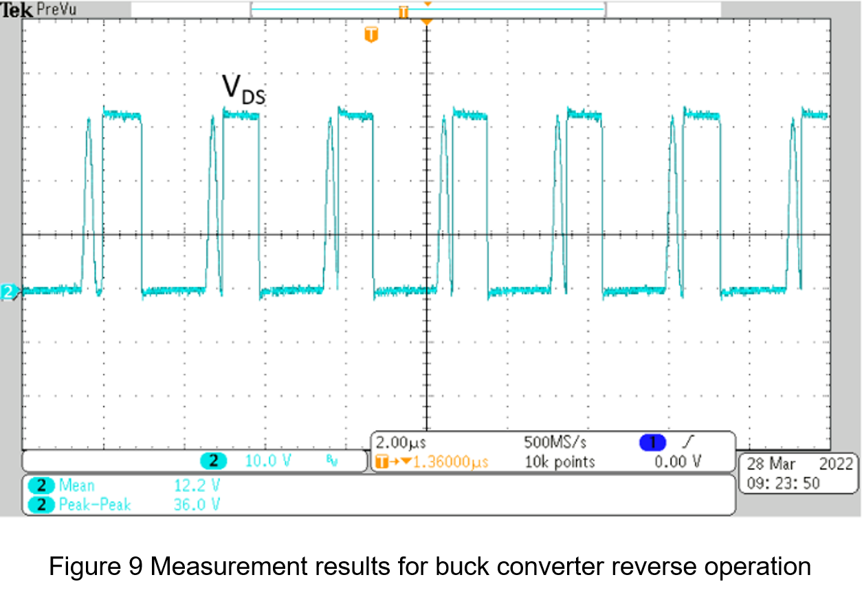
From this experiment, we know that the allowable input voltage range during normal operation is larger, as shown in Figure 8, VDS is 33.6V at an input voltage of 32V during normal operation. Figure 9 shows that in reverse operation, VDS reaches 36V at an input voltage of 20V, so attention must be paid to the withstand voltage of the internal components when reversing the output.
5. Efficiency
Since the input current when the positive and negative terminals of the buck converter are reversely connected will be greater than the input current in normal operation, the efficiency of the reversed output will be lower than that in normal operation.
Table 1 shows the measured data for the normal operation of the buck converter.
| Vin | Iin | Vout | Iout | η |
| 15V | 0.8237A | 11.96V | 0.9997A | 0.9676 |
| 20V | 0.628A | 11.977V | 0.9997A | 0.9532 |
Table 2 shows the measurement data for the buck converter output with positive and negative reversal.
| Vin | Iin | Vout | Iout | η |
| 15V | 0.9022A | -11.99V | 0.9997A | 0.8857 |
| 20V | 0.6598A | -11.99V | 0.9997A | 0.9083 |
6. Conclusion
It is possible to reverse the positive and negative outputs of the buck converter to produce a negative output voltage, but there are some special considerations that need to be taken into account in its use, such as the additional loss of efficiency due to the inductor current ripple, the output load current should not exceed half load and the poor conversion efficiency. Most important of all, reversing the output of a buck converter to a buck-boost converter at the same input voltage will result in the internal components being subjected to very different voltage stresses. Therefore, the operable input voltage range will be reduced depending on the actual input and output voltage settings at the time.
CTC is a professional service provider for high-end power supply modules (AC to DC Converter and DC to DC Converter) for critical applications worldwide since 30 years. Our core competence is to design and deliver products with leading technologies, competitive pricing, extremely flexible lead-time, global technical service and high-quality manufacturing (Made In Taiwan).
CTC is the only corporation certificated with ISO-9001, IATF-16949, ISO22613(IRIS), and ESD/ANSI-2020. We can 100% ensure not only the product, but also our workflow and service to match quality management system for every high-end application from the very beginning. From design to manufacturing and technical support, every single detail is operated under highest standard.

