

You are here
Back to topPCB Layout and Heat Dissipation Technology
Modern electronic products often use high-power electronic components. With the trend of smaller high-power components, the heat generated by high-power components is more difficult to dissipate, so the circuit temperature will rise rapidly. If the heat is not dissipated in time, the electronic components May be damaged by overheating. Therefore, solving the problem of heat dissipation is a very important issue when designing a circuit board. This article introduces several PCB layouts that can improve the heat dissipation, and measures the temperature performance of the power converter placed on different board layouts to observe the impact of different layouts on the heat dissipation effect.
1. PCB Thermal Design Analysis
The heat source of PCB is the power loss of components, and the amount of heat is proportional to the power consumption. The power consumption of the PCBs is analyzed from the following aspects, and corresponding measures is taken through these aspects to achieve the purpose of improving the heat dissipation capacity.
- Hot Spot Analysis
It is a particularly much high temperature on the PCBs, usually where high power components are much dense because that heat dissipation is difficult and large current flows. During design PCBs stage, the thermal model and thermal dynamic model can be used to simulate hot spots area occur, and the hot spot temperature can be reduced by changing layout planning or selecting suitable components.
- Layout
High current is one of the main causes of heat generation on the PCBs, planning the position of high-power components and copper foil lines makes the heat energy evenly distributed on the PCBs, which helps to avoid local high temperature. At the same time, it should be noted that the layout of high current path should avoid thermally sensitive components.
- Temperature Distribution
In practical applications, a thermal imaging camera or thermocouple wire can be used to observe the overall temperature distribution of the PCBs, and compare two methods with the simulated hot spot analysis. Finally, corresponding solutions for high-heating components. In this experiment, thermal imaging camera will be used to observe the temperature performance of the PCBs.
2. Methods To Reduce Circuit Board Heat
After analyzing the main causes of heat generation on PCBs, the following methods can be used to improve heat dissipation capacity, and thus increase conversion efficiency.
- Increase Area
The bottom plate of the PCBs is mostly made of copper-clad epoxy glass cloth or phenolic resin glass cloth. Those material have poor heat-dissipation effect, so only a small part of the heat energy is dissipated from the surface of the component to the surrounding. In order to improve the heat dissipation performance of the PCBs, the common method is to increase the copper clad and the size of the PCBs, but it must pay attention to the problem of electromagnetic interference.
- Add External Equipment
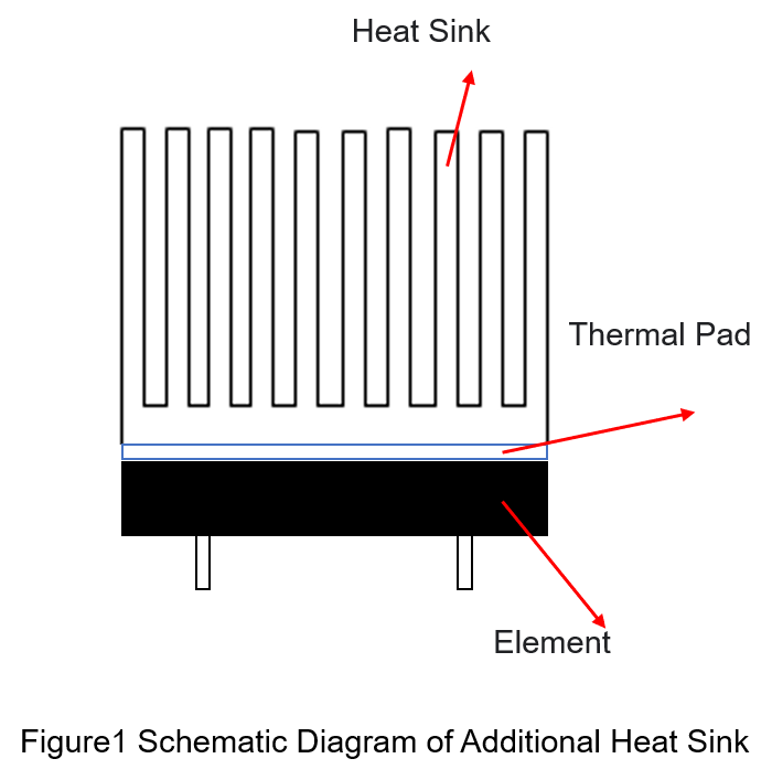
high heat generation components, such as power converters, high-power transistors, and CPUs. will be installed heat sinks to increase the heat dissipation area or fans to enhance air circulation, in addition, thermal pads can be used to fill the gap of contact surface between the heat sink and the high-temperature element, it can reduce heat thermal resistance between the source surface and the heat sink. Figure1 is a schematic diagram of adding heat sinks to components
- Component Layout
According to the heat energy of components and the degree of heat dissipation, low heat components such as capacitors, small-scale integrated circuits, should be placed in the upstream of the cooling air flow, on the contrary, high heat resistance components, such as power transistors and transformer, should be placed in the downstream of the cooling air flow to avoid to damage other components. Furthermore, high-heat components should be placed in the center of the PCBs or installed with heat dissipation devices as much as possible.
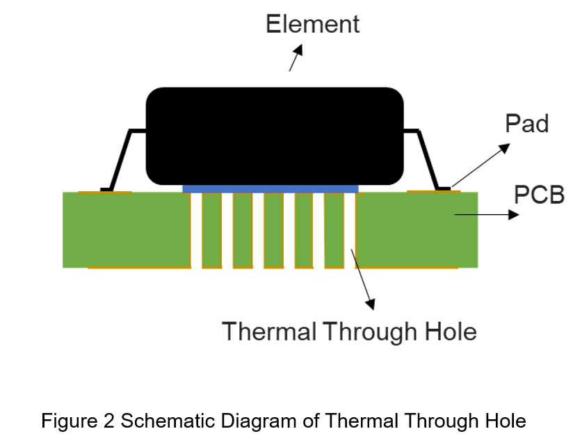
- Thermal Through Hole
Adding thermal through hole in PCB can to increase the thermal conduction paths, and the purpose is to reduce thermal resistance. In terms of a single-layer double-sided PCBs, the metal through hole can connect the surface and the copper foil on the back, and conduct the thermal energy of the front components to the back side. transmitted to the back of PCBs, as shown in Figure 2. The heat dissipation effect depends on the area and thickness of copper foil, the thickness and material of the PCBs. The thermal through hole is as close as possible to the heating element to achieve the best effect.
- Wire Layout Design
Adjusting the metal-line layout can strengthen the heat dissipation, for example, increasing the line width of the high temperature component, and reducing the metal-line length and avoiding right-angle traces. It can reduce noise interference and impedance, thereby improving the heat dissipation.

3. Actual Measurements
- Experiment 1: Comparison of Converter is Fixed or Not
The following will use a step-down DC-DC converter to compare the temperature differences between whether converter case is fixed or not in the wind tunnel, and the experimental specifications are as follows.
| Input Voltage | 48 V |
| Input Current | 3.125A |
| Output Voltage | 12 V |
| Output Current | 12.5 A |
| Output Power | 150 W(100% Load) |
| Input capacitor | 200uF |
| Wind Velocity | 100 LFM |
The power converter uses in the experiment a step-down DC converter with a rated power of 150W, with the 48V input and the 12V output.
Figure 4 is a photo of the aluminum-based housing fixed on the PCB by screws and taken with a thermal imager camera. It can find that the heat energy of the converter is conducted through the copper cladding of the PCB below, and evenly distributed in the copper coverage area. In result, it can be seen that increasing the PCB size and copper clad area can effectively improve the heat dissipation effect; the converter input and the output pin has a higher temperature performance because that the large current flowing through the pin generates a large amount of heat energy. The measured PCBs temperature is 103 °C, and the maximum temperature of the converter housing is 111 °C.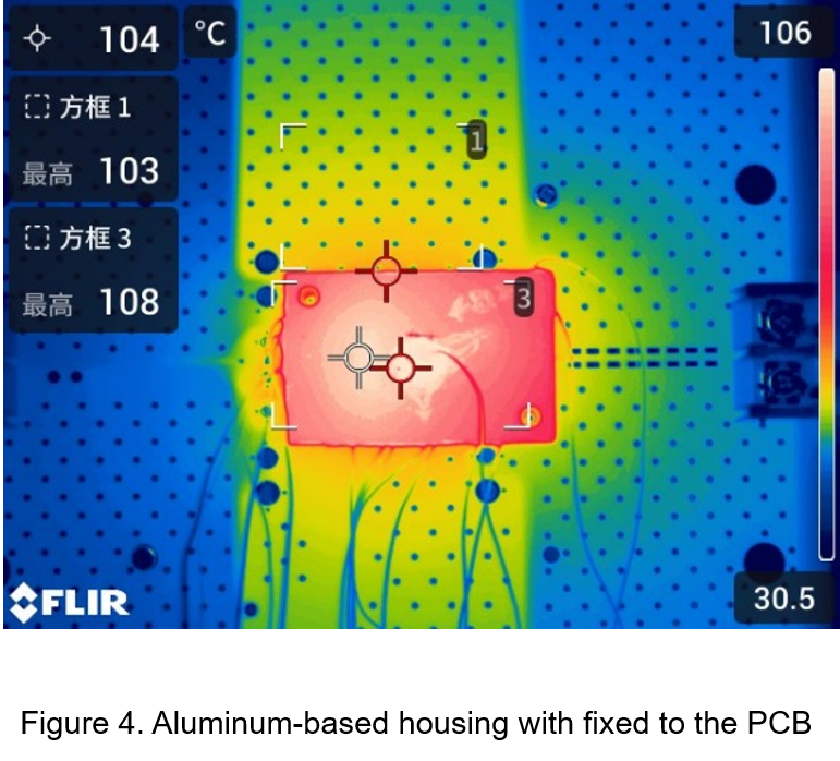
Figure 5
is a photo of the aluminum base housing not fixed on the PCB and taken with a thermal imager. Comparing to Figure 4 , the PCB temperature closing to the aluminum-based housing can be found to be higher because the thermal energy only be radiated possible and cannot be transmitted to the PCB through contact. Therefore, the pins soldered on the PCB become the main path for heat transfer. This maximum temperature in figure 5 is higher at the input and output ends than in Figure 4 . The measured temperature of the PCB is 111 °C, and the maximum temperature of the converter housing is 118 °C.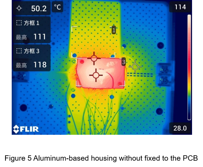
- Experiment 2: Comparison of Different Size PCBs
The converter outer casing is fixed on the PCB with screws, and the wind speed is changed from 100LFM to 20LFM. The smaller wind speed can more clearly compare the heat dissipation capacity difference between the different size of PCBs. The experimental specifications are shown in Table 2.
| Input Voltage | 48 V |
| Input Current | 2.813A |
| Output Voltage | 12 V |
| Output Current | 11.25 A |
| Output Power | 135 W(90% Load) |
| Input capacitor | 200uF |
| Wind Speed | 20 LFM |
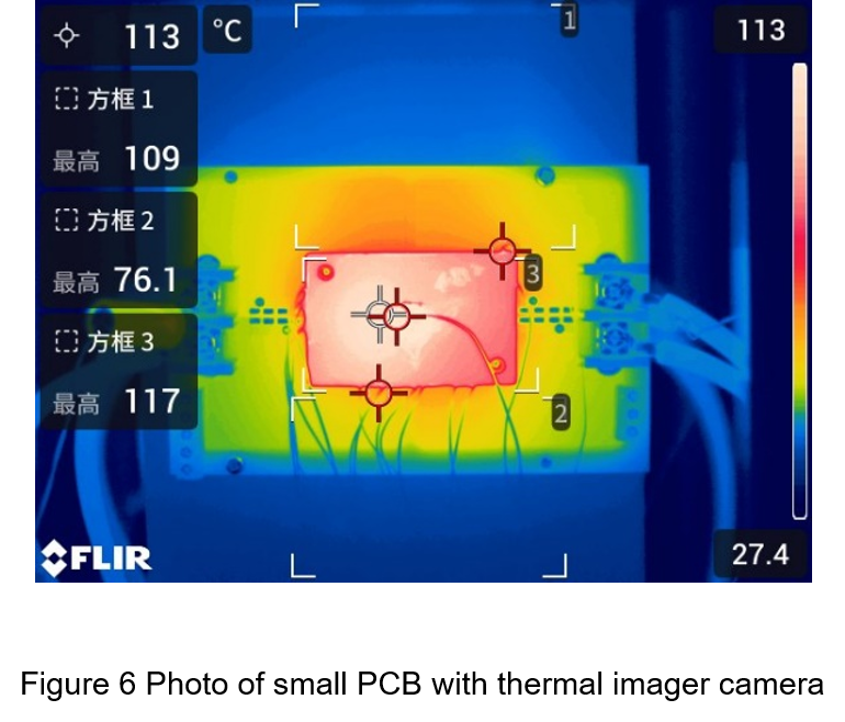
Figure 6
is a photo of a small PCB with thermal imaging camera at 90% load. It can be seen that the heat dissipation area of the printed circuit board is too small, and it is impossible to dissipate the heat energy of the converter immediately, so the overall temperature will continue to rise. From the experimental results, the temperature of converter case is 117 degrees at 90% load, and the edge of the converter is about 109 degrees, which shows that the heat dissipation capacity of the small PCB is limited.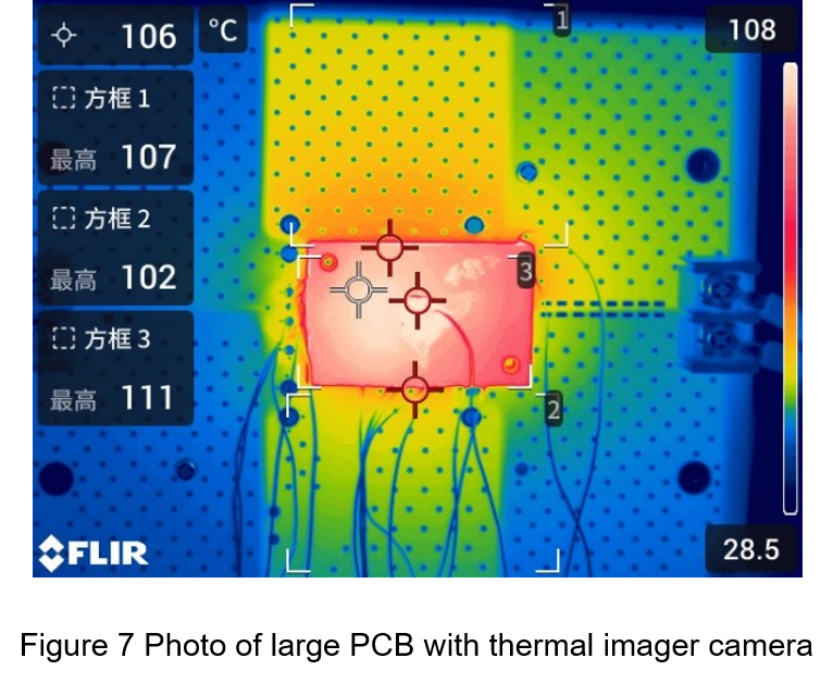
Figure 7 is a photo of a large PCB, about triple size with thermal imaging camera at 90% load. Since its copper cladding area is larger than small case and some thermal through hole are arranged, the temperature performance is better. From Figure 7, it can be found that the maximum temperature of the converter case is 111 degrees, and the edge temperature is 107 degrees. It can be seen that the heat dissipation capability of the circuit board can be improved by increasing the copper clad area and increasing the thermal through hole.
Conclusion
With the development of surface mount technology, how to solve the heat dissipation problem caused by high power density is a key factor. An excellent layout not only can reduce temperature range but also improve conversion efficiency, which will extend the service life of converter. From the experimental results, it can be known that the heat energy will be more effectively dissipated to the surroundings of the PCBs through thermal through hole. Thus, improving the heat dissipation ability and the overall conversion efficiency.
CTC is a professional service provider for high-end power supply modules (AC to DC Converter and DC to DC Converter) for critical applications worldwide since 30 years. Our core competence is to design and deliver products with leading technologies, competitive pricing, extremely flexible lead-time, global technical service and high-quality manufacturing (Made In Taiwan).
CTC is the only corporation certificated with ISO-9001, IATF-16949, ISO22613(IRIS), and ESD/ANSI-2020. We can 100% ensure not only the product, but also our workflow and service to match quality management system for every high-end application from the very beginning. From design to manufacturing and technical support, every single detail is operated under highest standard.