

You are here
Back to topDC to DC Converter Protection : Under Voltage Lock-out
Most electronic converters include an undervoltage lockout (UVLO) function, to disable the converter when the input power source is at low supply voltage and protect the device from damage.
When the supply voltage is too low and without relevant protection, the function and performance of converter may be undefined. For example, the logic circuit could be malfunction, or the MOSFET will operate in linear region mode instead of saturation mode, which will cause a large amount of heat in the MOSFET, and eventually cause damage. This is especially important in battery powered applications because the voltage of the battery will decrease during the discharge process. If there is no appropriate protection, it will not only damage the converter, but also the battery module.
Figure 1 shows the operation mode of the converter at different input voltages. It can be roughly divided into two blocks. The left half is the input voltage startup and the right half is the input voltage cutoff.
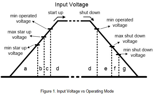
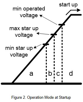
The startup portion can be divided into four operating modes.
- When the input voltage is below the minimum startup voltage, the converter has no output, as shown in Figure 2 block a. The input current is usually very low at this status.
- There are some tolerances when setting parameters. The difference may come from components or temperature variations. When the input voltage is between the lowest and highest startup voltages, as in block b of Figure 2, the converter cannot determine if it has started normally.
- When the input voltage exceeds the maximum startup voltage, but still has not reached the minimum operating voltage, as shown in Figure 2 block c. At this condition, the converter has started, but not suitable for full load output because the input current may be too large.
- When the input voltage is higher than the minimum operating voltage, the converter operates normally, as shown in Figure 2 block d.
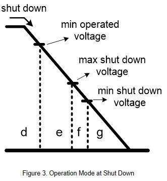
The shut down portion can be divided into four operating modes as well.
- The converter operated normally in Figure 3 block d.
- When the input voltage is lower than the minimum operating voltage, but still higher than the cutoff voltage, as shown in Figure 3 block e. The converter is not turned off. But in this condition, converter is not suitable for continue full-load output. The reason is that the input voltage is insufficient, causing the output voltage to be lower than the nominal voltage of the specification.
- Figure 3 blocks f is the same as Figure 2 block b. There are some tolerances when setting parameters. When the input voltage is between the highest and lowest cut off voltages, the converter cannot determine if it has been normally turned off.
- When the input voltage is lower than the lowest cutoff voltage, the converter shut down, as shown in Figure 3 block g. The input current is usually very low under this condition.
Design Guide Line
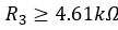
Figure 4 shows the circuit diagram for UVLO. The EN pin controls the operation status of the converter. The purpose of the circuit is to detect the input voltage value through the IC and control the operation status of the converter. As shown in Figure 3, IC1 detects the input voltage level through R1, R2 and R3. The converter will start up normally when the input voltage is higher than the setting value. When the voltage level on R3 is lower than the setting voltage of IC1, the switch inside IC1 will turn on, pulling the EN pin to low level, and shut down the converter.
Assuming the voltage level on R3 is higher than the setting voltage, the switch inside IC1 is turned off. The EN pin is floating, the converter can operating normally.

For example, if the converter start up voltage is 8V, and the IC1 setting voltage is 2.5V. The IC1 will detect the divided voltage by R1, R2 and R3. The formula as follow
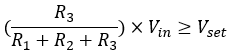
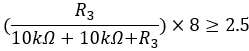
The result is
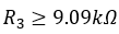
In addition, it should be noted that when the input voltage reaches the maximum value, the voltage of IC1 cannot exceed the upper limit of the specification. Therefore, the voltage between R2 and R3 can be clamped by a zener diode. For example, the IC1 max setting voltage can't exceed 5V. Through the partial formula, the voltage on ZD1 can't exceed 10.5V. In this case, ZD1 must use 10V zener diode.
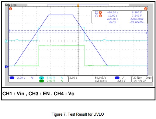
Another type of UVLO circuit can refer to Figure 5. The operation principle is when the input voltage reaches the setting value, the Q2 switch turns on and provides the normal operated voltage to converter.
As shown in the Figure 5, the initial status of Q1 is off. When the Q2 is turned on, pulling the Q1 Vgs voltage level to low level, the Q1 can then be turned on. Whether Q1 is turned on or off is determined by setting the voltage division values of R1, R2, and R3.

For example, assuming the converter start up voltage is 8V, and the Q2 Vgs level is 1.5V. Through divide voltage by R1, R2 and R3, the formula as follow
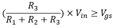
If the R1 and R2 resistors are 10kΩ and are brought into the formula.
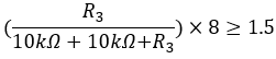
The result is
ZD1 clamps the Vgs voltage of Q1 within the specification value. The C1 is to avoid noise interference and increase the start-up time of Q1, reducing the surge current at startup.
Example
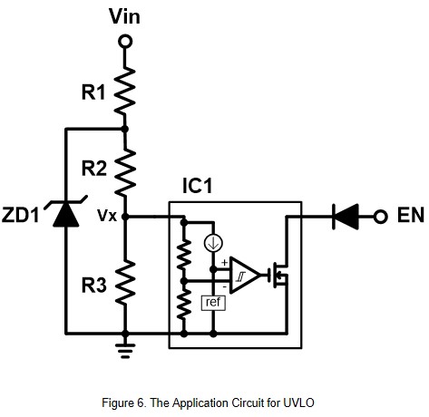
Next step, using the application circuit of Figure 6 and the converter to simulated the UVLO function. First of all, assuming the converter turned off voltage is about 7.5V, and the IC setting voltage is 2.3V. After calculation by the formula, the parameter can be obtained, R1=100kΩ, R2=88.7 kΩ, R3=82 kΩ. And then, brought the parameters back to the formula, and we can get the converter start up voltage is about 8.5V.
The test waveform is shown in Figure 7. When the input voltage climbs from 0V up to the setting voltage, the UVLO circuit will turn the converter off. When the input voltage reaches 8.4V, which is the setting voltage, the converter operates normally. When the input voltage drops to 7.84V, the UVLO circuit will turn off the converter, to avoid the converter been damaged by the excessive input current.
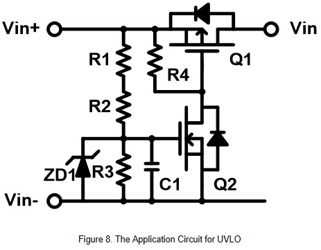
The input voltage of the converter can also be controlled by the external circuit of figure 8. First, assume the converter shut down voltage is 10.5V. The Q2 Vgsth minimum is 1V, maximum is 2.5V, and normal state is about 1.5V. After calculation by the formula, we can get R1=100kΩ, R2=100 kΩ, R3=30 kΩ, and bring back the formula to get the start up voltage is about 11V.
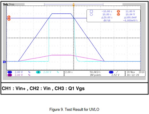
The test waveform is shown in Figure 9. When the input voltage rises from 0V to the setting voltage, Q1 is off. And the converter has no input and output voltage. When the input voltage reaches 11V, Q1 turns on and the converter operates normally. When the input voltage drops to 10.84V, the UVLO circuit turns Q1 off and the converter is turned off as well.
Summary
Converters with UVLO feature will not operate when the input voltage is still established or has not reached the stable stage. This has the advantage that the input supply can almost completely charge the input capacitance of the converter, which can reduce the input voltage drop caused by the converter startup. In addition, the converter can also turn off the converter before the input voltage drops to a certain value, to avoid damage to the converter causing by excessive input current.
CTC is a professional service provider for high-end power supply modules (AC to DC Converter and DC to DC Converter) for critical applications worldwide since 30 years. Our core competence is to design and deliver products with leading technologies, competitive pricing, extremely flexible lead-time, global technical service and high-quality manufacturing (Made In Taiwan).
CTC is the only corporation certificated with ISO-9001, IATF-16949, ISO22613(IRIS), and ESD/ANSI-2020. We can 100% ensure not only the product, but also our workflow and service to match quality management system for every high-end application from the very beginning. From design to manufacturing and technical support, every single detail is operated under highest standard.