

You are here
Back to topHow do I reduce the Inrush Current?
Apr 09, 2020
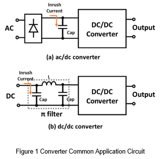
In order to reduce the input or output ripple noise or EMI noise, current power converter usually connected in parallel with capacitors or filter at the input side, as Figure 1 show. The filter usually composed of an inductor or capacitor. Because there is capacitor in the filter, when the system is initially powered, a high surge current will be generated due to the rapid rise of input voltage. Such a situation may cause the front-end power supply to be insufficient, causing the output voltage of front-end power supply insufficient, or to trigger the over current protection, resulting in no voltage output. So, the suppression of inrush current is becoming more and more important feature.
1. Introduction
1.1 Passive Suppression
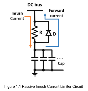
Figure 1.1 is another type of inrush current limiter circuit, which is mainly used when the application circuit needs large number of external capacitors. If there is no external current limit circuit, it will generate a large surge current when the DC bus voltage turn on, which may cause the front-end power supply voltage drop or enter protection mode. At this time, just to connected resistor and diode in series with the capacitor input side. The inrush current can be alleviated. When DC bus is charging to the capacitor through resistor, so the inrush current can be limit. However, when the DC bus needs power, the capacitor can fed the power back to the DC bus through diode.
1.2 Active Suppression
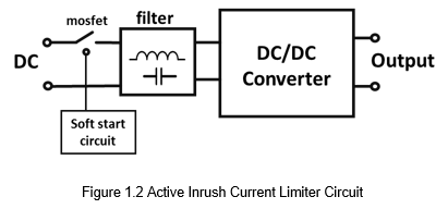
The other is to use an active switch with soft start circuit to limit the inrush current, as shown in Figure 1.2. The MOSFET turn on slowly by soft start circuit. Therefore, the inrush current can be limit during start up. The advantage is it does not affect the efficiency of the system and is not affected by the ambient temperature. The disadvantage is that it needs to connect additional circuit and the overall cost is higher.
2. Inrush Current Limiter Circuit
As previously content, there are two methods to limit inrush current, each with its own advantages and disadvantages. The active inrush current limit uses the turn on resistance of the MOSFET during startup to suppress the input current. Furthermore, because the conduction loss of the MOSFET is low and it is easy to used. So, to using MOSFET to limit the inrush current is very common. The advantage of passive method is fewer parts, but the disadvantage is it still has power loss. The following will introduce active and passive inrush current limiter circuit.
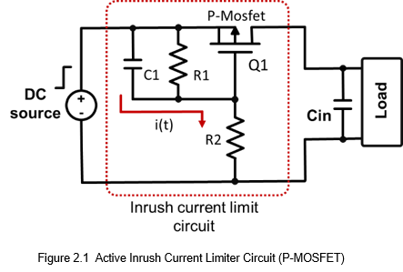
2.1 Active Inrush Current Limiter Circuit (P-MOSFET)
Figure 2.1 shows the inrush current limit circuit by using P-channel MOSEFT. The P-channel turn on step basically is same with N-channel, but the voltage is opposite. In the initial stage the voltage on C1 is 0V.
The input voltage is charged to C1 through R2. Finally, the voltage on C1 is determined by dividing the voltage between R1 and R2.
The Q1 turn on status is determined by the Vgs voltage.
- -Vgs<-Vgs(th) and -Vgd<-Vgs(th)
The MOSFET is in cutoff state, which is similar to an open circuit.
- -Vgs>-Vgs(th) and -Vgd>-Vgs(th)
The MOSFET is in the ohmic mode. The characteristic of Vds and Id is like a resistance, and it becomes smaller as the Vgs voltage increases.
- -Vgs>-Vgs(th) and -Vgd<-Vgs(th)
The MOSFET is in a saturation mode. Id is a fixed value and does not change with Vds. And the MOSFET turn on resistance is very low, which is suitable for switching.
From the depiction of MOSFET's characteristic, the ohmic mode is most suitable for suppressing inrush current. As for the calculation of R1, R2, and C1, it can use the following formula:


The values of R1 and R2 can be obtained through Equation 8, and C1 and the startup time can be obtained through Equations 1 and 3. Under the same R1, the larger C1, the longer the MOSFET operates in the ohmic mode, which means that the effect of limiting inrush current will be better.
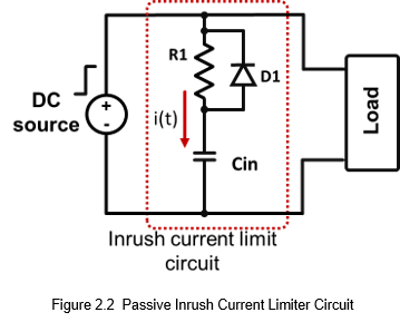
2.2 Passive Inrush Current Limiter Circuit
The general passive method is to connect a thermistor in series at the input. But because the thermistor is greatly affected by the ambient temperature, there will be no protection when the ambient temperature is high or the input power supply is quickly opened and closed many times.
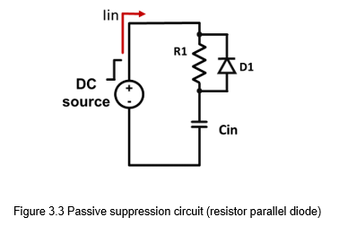
The Figure 2.2 shows the circuit which can improve this phenomenon. The use diode and resistor connect in parallel, and connect in series with the capacitor. Can not only suppress the inrush current, also they are no easily affected by temperature changes or input power quickly opened and closed many times.
The operating principle is that when there is input voltage, the input voltage charges Cload through R1, and when the system load needs power, Cload discharges to the load through the diode.
It can be seen from the figure that R1 is inversely proportional to the inrush current, so it can be calculate R1 by the following formula:


Loss on R1

t Can be roughly regarded as a double time constant

Loss of resistance can be obtained by taking formula (6).
3. Application
3.1 Active suppression circuit (P-channel MOSFET)
Make an inrush current suppression circuit according to Figure 3.1, and use the formulas (1) to (4) to calculate the circuit parameters.
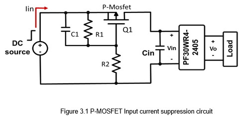
| Q1 | AP9120GH |
| R1 | 10 kΩ |
| R2 | 20 kΩ |
| C1 | 1 uF |
| TYpe | Vdss | Vgs(th) | Rds(on) | Id |
| AP9120GH | -200 V | -2~-4 V | 0.68 Ω | -8 A |
Experimental conditions
The following table shows the specifications of the DC-DC power converter used in this experiment.
| DC to DC Converter | PF30WR4-2405 |
| Input voltage | 24 Vdc |
| Output voltage | 5 Vdc |
| Output current (full load) | 6000 mA |
| Cin | 220 uF |
Experimental results
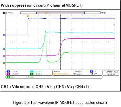
Figure 3.2 is the test waveform of the P-MOSFET suppression circuit. It can be seen from the figure that the input surge current is effectively suppressed. At the same input voltage and input capacitance, the surge current is suppressed from 122 A to 4.546A.
3.2 Passive suppression circuit
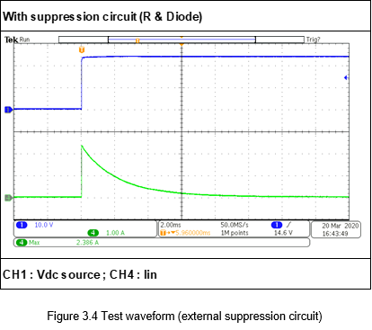
An inrush current suppression circuit is according to Figure 3.3, and the parameters are calculated in accordance with formula (6).
Experimental conditions
| Input Voltage | 24 Vdc |
| R1 | 25 Ω |
| D1 | V10P10 |
| Cin | 220uF |
Experimental results
Figure 3.4 is a test waveform using a resistor and diode suppression circuit. At the same input voltage and input capacitance, the surge current of the input capacitor is suppressed at 2.386A.
3.3 Passive suppression circuit
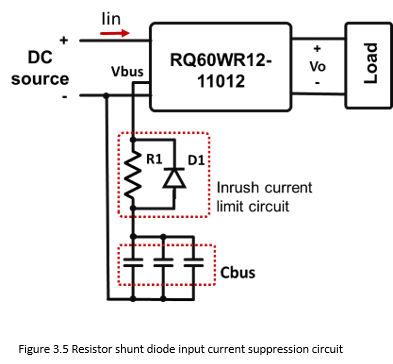
In railway applications, the input power maybe interrupted or unstable due to vibration or when the cabin is connected to each other. At this time, the power modules must maintain stable operation under such circumstances. Therefore, a common method is to connect large number of capacitors at the input side to maintain a stable output, as shown in Figure 3.5. But, lot of capacitors means high inrush current might be appeared. So, passive suppression circuit is very suitable for this.
Experimental conditions
| DC to DC Converter | RQ60WR12-11012 |
| Input voltage | 24 Vdc |
| Output voltage / Current | 12 Vdc / 5000 mA |
| Cbus | 800 uF |
| R1 | 24 Ω |
| D1 | SVC4200VB |
Experimental results
Figure 3.6 is the test waveform without external suppression circuit. From the figure, you can see that the input surge current is as high as 24.13A.
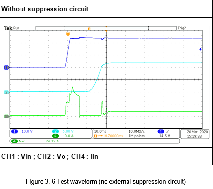
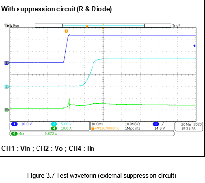
Figure 3.7 is the waveform tested by using the suppression circuit. The illustration can grind the input surge current to be effectively suppressed, leaving 9.67A.
Conclusion
In order to strengthen the anti-noise ability of DC/DC converters, the common method is to add capacitor at the input side. However, due to the characteristics of the capacitors, inrush current is caused at the input side of the power supply. If the inrush current is not suppressed, the input power might have no output due to protection circuit, and it maybe damage the input circuit or fuse.
This article introduces two inrush current suppression methods, one is using MOSFET’s turn on characteristics to suppress inrush current. The other is using passive components, which charge the capacitor through a resistor and then discharge it back to the system through diode. The result of active suppression circuit is better than passive one, but the part count is more than passive suppression circuit. The components of the passive suppression circuit use the least, but the loss and power selection of the resistor must be considered. From design to verification results, both methods can effectively suppress inrush current. The use of passive or active suppression of surge current is the trend of future power supply design.
CTC is a professional service provider for high-end power supply modules (AC to DC Converter and DC to DC Converter) for critical applications worldwide since 30 years. Our core competence is to design and deliver products with leading technologies, competitive pricing, extremely flexible lead-time, global technical service and high-quality manufacturing (Made In Taiwan).
CTC is the only corporation certificated with ISO-9001, IATF-16949, ISO22613(IRIS), and ESD/ANSI-2020. We can 100% ensure not only the product, but also our workflow and service to match quality management system for every high-end application from the very beginning. From design to manufacturing and technical support, every single detail is operated under highest standard.