

You are here
Back to topSelection Guide for SiC MOSFET Gate Drive Voltage
In high-power applications, power transistors are often used as switching elements for drive. Selecting an appropriate gate drive voltage can greatly reduce switching losses, so gate drive voltage range is one of the important factors. This article explains how to design the gate drive voltage of a power transistor to achieve optimal performance and reliability.
Introduction
In recent years, the electric vehicle market has performed outstandingly. Since then, tens millions of electric vehicles have been driven on the road. It can be seen that the sales of electric vehicles have grown significantly. In this application, gate drivers are required for many electronic devices, such as traction inverters, on-board chargers. In order to effectively drive the power transistor, selecting an appropriate gate drive voltage can reduce the risk of instantaneously high driving voltage and reduce switching loss, which means to have a shorter switching time.
Figure 1 is the common buck converter architecture. The two power transistors Q1 and Q2 on the system are the high-side driver switch and the low-side driver switch, respectively. The positive/negative drive voltages for both driver switches are determined by the isolated converter.

With the demand of terminal markets dramatically increasing, many electronic product designs use silicon carbide (SiC) wide-gap semiconductor materials as power transistor, which can provide lower switching losses, higher switching frequency and operating temperatures than traditional silicon metal oxide semiconductor field-effect transistors. Therefore, how to determine the gate driving voltage of the SiC MOSFET is an important issue.
How to Select the Gate Drive Voltage
To efficiently turn on and off power transistors, it is necessary to select right driving voltages for various types of power transistors. Table 1 shows the driving voltages of various type power transistors.
|
Type |
Si-MOSFET |
IGBT |
SiC |
GaN |
|
Turn on Voltage |
10V to 20V |
15V |
15V to 20V |
5V to 6V |
|
Turn off Voltage |
0V to -2V |
-5V to -15V |
-2V to -5V |
0V to -3V |
|
Common Drive Voltage |
+12V/0V |
15V/-9V |
15V/-3V |
5V/0V |
| - |
15V/-5V |
15V/-5V |
6V/-3V |
In practical applications, in order to fully turn on the power transistor, positive voltage of gate drive needs to be high enough, and cares that it should be taken not to exceed the rated voltage of the gate; in addition, negative voltage uses to turn off the power transistor to quickly enter the cut-off region. The reference potential of the converter is affected by the noise of the parasitic inductance and capacitance of the PCB when switching the switch, causing circuit malfunction.
When designing, it is necessary to pay attention to the positive/negative drive voltage must not exceed the maximum gate-source voltage rating, once the voltage overs withstand the limit, reliability problems of component such as deterioration and damage may occur. For example, the positive drive voltage of common SiC components of 15V cannot be applied to GaN components; The negative drive voltage of -15V for common IGBT components also cannot be applied to GaN components.
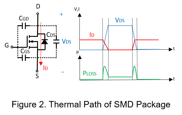
One problem is switch loss, the power transistor will be in a state of high voltage and high current at the same time in a short period of time when switching, so that the parasitic capacitance will continue to be charged and discharged in the process. If it continues in this state for a long time, more energy led to be consumed. In order to reduce the switching loss, the duration of this stage should be minimized, as shown in Figure 2.
Another problem is the internal gate resistance. Once the on-resistance of the power transistor is higher, more heat will be generated inside the system, which can lower the power conversion efficiency. So how to reduce the on-resistance? In terms of SiC MOSFET process characteristics, the higher the difference of gate-source voltage, and the lower the on-resistance; the lower the temperature, and the lower the on-resistance, as shown in Figure 3.

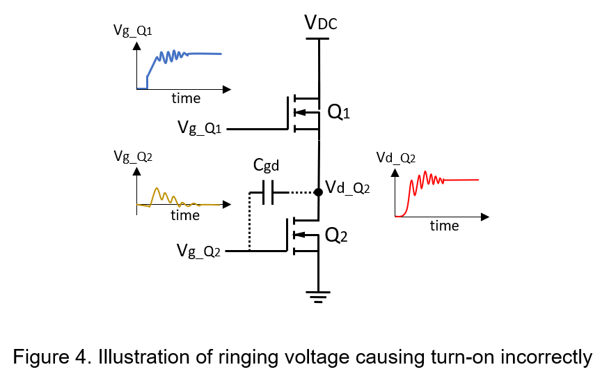
The following briefly discusses how to determine the driving voltage of SiC MOSFET. When the common positive driving voltages are 12V, 18V and 20V, which voltage should be selected? Because the Vgs-Ron curve of common SiC MOSFETs shows that the on-resistances of the driving voltage 18V and 20V are quite small and low difference each other. But it can use driving voltage 18V to reduce the possibility of damage to components by surge effect; In addition, when the common negative driving voltages are 0V, -3.3V and -5V, which voltage should be selected? While all can turn off the power transistor, the possibility of turn-on incorrectly needs to be considered. It means that gate drive voltage (dVg/dt) of Q1 changes quite fast, lets drain voltage of Q2 to ring, which is coupled to the gate drive voltage of Q2 through parasitic gate-drain capacitance. If the ringing voltage exceeds the threshold voltage of Q2, large current flows directly through Q1 and Q2, which can reduce conversion efficiency or even destroy components.
For example, the threshold voltage of Q2 is 2.8V and the maximum ringing voltage is 3.5V. If the gate drive voltage is -5V, the gate-source voltage of Q2 is
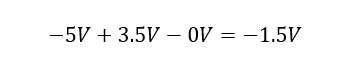
This result is significantly lower than the threshold voltage. It can be seen that when the gate drive voltage is negative instead of 0V, , the gate-source voltage cannot be higher than the threshold voltage even if affected by ringing voltage . Therefore, selecting negative voltage to turn off SiC. MOSFETs is preferred.
It can use a large positive gate drive voltage to charge the gate capacitor, so as to reduces switching loss and conduction loss; Moreover, it uses a smaller negative gate drive voltage to quickly release the charges of gate capacitor to avoid ringing and cause power transistor to conduct incorrectly.
Conclusion
In recent years, third-generation semiconductors are often used as high-voltage and high-current switches. The design of gate-source voltage needs to consider factors such as power consumption and system reliability. This article introduces that selecting the driving voltage needs to be considered to avoid the driving voltage exceeding the maximum rated voltage, reducing the energy loss of the switch and large on-resistance of the power transistor.
CTC is service provider for high-end power modules (DC to DC Converter and AC to DC Converter) for critical applications worldwide since 1987. We aim to be business generator and a virtual business unit. CTC is your own team with 35 years of experience for a strong business program from market research, product definition & development, supply chain management and total technical services.
CTC is the only corporation certificated with ISO-9001, IATF-16949, ISO22613(IRIS, AFNOR silver certificate), and ESD/ANSI-2020. We can 100% ensure not only the product, but also our workflow and service to match quality management system for every high-end application from the very beginning. From design to manufacturing and technical support, every single detail is operated under highest standard.