

You are here
Back to topRecommended Converter PCB Layout – Heat Dissipation Part I
Printed circuit boards (PCBs) have been widely used in various electronic products. In high-power applications, heat energy is required to be quickly transferred to the surface of the PCB, so that the overall system can maintain high-efficiency. Therefore, solving the heat dissipation problem is a very important step when designing PCB. This article introduces the influence of different copper thickness and area on the heat dissipation of the PCB. It also measures temperature of the power converter not placed on PCB, and placed in different PCB layouts, then observes the temperature distribution through infrared thermal imager.
Introduction
With the trend of increasing power density and miniaturization of consumer electronics products, all active and passive components are placed closer. If there are high current components flowing inside the power converter (such as power transistors, transformers, resistors), a large amount of heat energy is emitted and cannot be quickly transferred to the surroundings for heat dissipation. At this time, the temperature of the PCB is too high until it exceeds the critical value, resulting in overall inefficient operation.
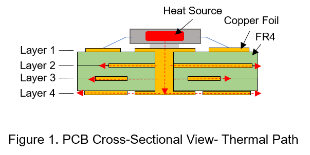
Generally, the thermal conductivity of PCB with multi-layer composite structures is anisotropic, and its materials are mainly composed of composite materials of epoxy resin glass fiber board (FR4) and metal copper foil, and the purpose of FR4 is to enhance insulation and heat resistance; Metal copper foil connects conductor the lines between electronic components and maintain the uniformity of the PCB surface temperature performance. The x-axis and y-axis thermal conductivity of FR4 is 0.9 W/(m K), and the z-axis thermal conductivity is 0.3 W/(m K), so PCB dissipated less heat energy in the horizontal direction than vertical direction, but above of values are both much smaller than the thermal conductivity of metal copper foil 385W/(m·K), so that PCB mainly dissipated by metal copper foil.
PCB Heat-Dissipating Capability
A common optimization of PCB’s trace design is to increase the thickness and effective area of metal copper foil to achieve better thermal conductivity.
- Effective Area of Copper Foil
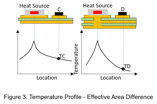
Many PCBs have a large area of copper because it can help to dissipate heat and anti-interference. If the temperature of heating element is too high and only rely on using heatsink to increase contact area, the heat dissipation effect is not enough for high power applications. Enlarging the single-sided copper foil area of the heating element can reduce the thermal resistance and discharge heat. But considering the be used PCB size, it can't unlimitedly increase the area. Improvement methods include that adding through holes on PCB copper foil around heat source. If through hole of double-layer board, it can connect the surface and back of PCB; if through hole of a multi-layer board, it can connect specified layers.
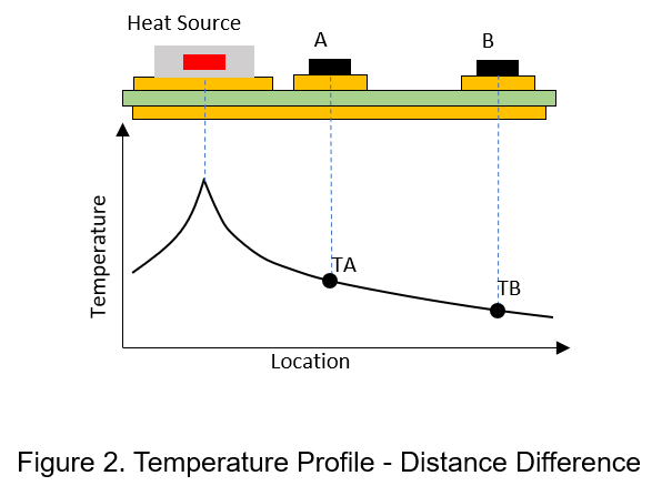
In natural convection environment, high-temperature components should be placed as far away as possible from heat-sensitive components such as thermistors, so as not affects the electrical characteristic due to local high temperatures. As shown in Figure 2, the farther away from the heat source, the less affected by temperature.
A through hole is placed on the surface and bottom of the PCB under high temperature component, and the bottom side is covered with copper. By the Thermal equilibrium, heat energy can be dissipated more easily through a larger area of metal copper foil.
- Copper Foil Thickness and Wire Width
Printed circuit boards mainly use metal copper foil to conduct heat, so what is the effect of different copper foil thicknesses and wire widths on heat conduction? The thickness of copper foil is generally measured in ounces(OZ), and the unit is 1oz/square foot. The thickness of copper foil commonly used in design is 1OZ (about 35µm), 2OZ (about 70µm) and 3OZ (about 105µm).
In high power application, the line impedance of current flowing through will generate heat due to conduction loss, so for high current loop, increase the thickness of the copper foil to reduce the line resistance, and the resistance of a wire can be expressed as

l : wire length (mm)
w: wire width (mm)
t: copper foil thickness (µm)
ρ: copper resistivity (µΩ)
Assuming that the current is uniform on the cross-sectional area of the wire, formula (1) is true only for direct current. It can be seen that the width of wire and the thickness of copper foil are inversely proportional to the wire resistance, but proportional to the heat dissipation capacity.

Experiment
The following will use isolated DC/DC converter to be placed on PCB with different metal copper foil thicknesses, and then infrared imaging camera detects and converts the thermal energy into electrical signals
. Thermal imaging is simply the process of converting infrared (IR) radiation (heat) into visible images that depict the spatial distribution of temperature differences in a scene viewed by an infrared camera, in order to find out the maximum temperature of PCB.
The power converter is a wide input voltage range from 9 to 36V input, a regulated 12V output, an output power of 30W, and an output current of 2.5A. The specifications are shown in Table 1.
| DC to DC Converter 661 | |
| Input Voltage | 24Vdc |
| Output Voltage / Current | 12Vdc/2.5A |
| Operating Temperature | -40~105°C |
| Case Temperature | Max.110°C |
| Wind Speed | 100LFM |
The experimental results are all measured with an input voltage 24V in full load, and the infrared image is captured when the power converter is in thermal equilibrium.
First, measure the temperature distribution of simple power converter itself without placing in PCB, and use alligator clips to directly clamp the input pin and output pin.
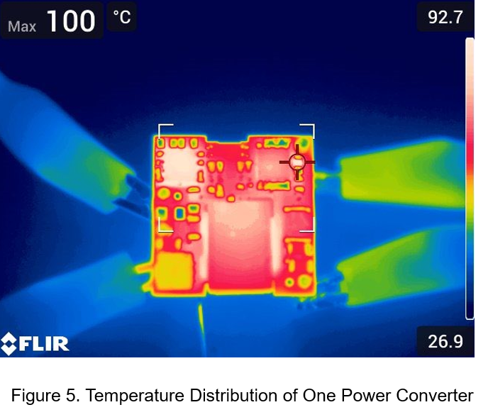
The input/output pins only dissipate heat through air and fixtures, so the efficiency of heat condution is poor. The highest temperature component detected is about 100°C.
- Thickness Difference of Copper Foil
Using the same PCB floorplan design, the power converters were placed on the PCB with copper foil thickness 2OZ and 3OZ respectively in order to measurement.
Figure 6 shows the temperature distribution of the copper foil thickness 2OZ. The maximum temperature of the PCB is about 39.3°C.
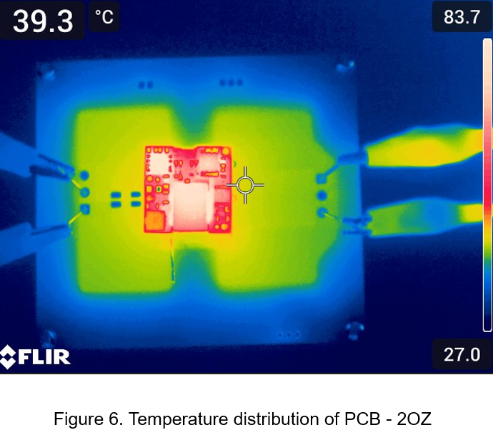
Figure7 shows the temperature distribution of the copper foil thickness 3OZ. The maximum temperature of the PCB dropped to about 35.1°C.
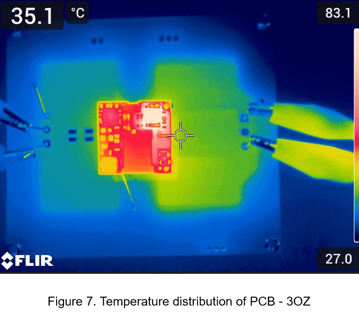
According to the above experiments, as the thickness of the copper foil increases from 2OZ to 3OZ, the temperature gradient of PCB decreases significantly, and the maximum temperature difference is about 4.2°C.
Conclusion
In order to evenly distribute the thermal energy generated by the large current loop on PCB, the efficiency of heat dissipation can be increased by enlarging the trace width and the copper foil thickness, and reducing the trace length. Considering the cost, it is necessary for the user to conduct thermal performance analysis of PCB before designing floorplan.
CTC is service provider for high-end power modules (DC to DC Converter and AC to DC Converter) for critical applications worldwide since 1987. We aim to be business generator and a virtual business unit. CTC is your own team with 35 years of experience for a strong business program from market research, product definition & development, supply chain management and total technical services.
CTC is the only corporation certificated with ISO-9001, IATF-16949, ISO22613(IRIS, AFNOR silver certificate), and ESD/ANSI-2020. We can 100% ensure not only the product, but also our workflow and service to match quality management system for every high-end application from the very beginning. From design to manufacturing and technical support, every single detail is operated under highest standard.