

You are here
Back to topRecommended Converter PCB Layout – Heat Dissipation Part II
Overheating of the printed circuit board (PCB) often leads to electronic circuit performance failure and reduced equipment reliability. This is why designers need to optimize PCB to improve overall system cooling, and thermal vias are one way to do this. This article explains the function of thermal vias and suggests how to configure thermal vias for heat dissipation rapidly.
Introduction
Today's popularity of wide bandgap semiconductors such as Silicon carbide (SiC) and Gallium nitride (GaN), which can enable power converters to achieve higher operating temperatures and output power. Therefore, thermal management is necessary to evenly distribute the generated thermal energy to avoid that the dangerous over-hot spots are generated.
The application article "PCB Layout Recommended by the Converter-Heat Dissipation Part I" mentions the heat dissipation area is increased through the through-holes of the printed circuit board, and then the copper foil layer dissipates heat to achieve a high-slope heat dissipation curve, ensuring that each component is kept at within safe temperature range, and the limit temperature specified in the manufacturer's data sheet should not be exceeded.
Placing thermal vias is a one way to effectively reduce thermal resistance for surface mount device. The thermal resistance is inversely proportional to thermal conductivity and the area of copper foil. Since the miniaturization of PCB area has become a basic requirement, there is no way to increase the copper layer area indefinitely, if there is not enough copper space on the top layer, it can use thermal vias to connect top copper layer to the bottom copper foil. The larger the heat transfer coefficient, the more heat transfer occurs, however, the heat transfer coefficient depends on a kind of the selected material. The following table shows the thermal conductivity of different materials.
| Material | Thermal Conductivity (W/mK) |
| Copper | 395 |
| Lead frame | 275 |
| Silicon | 146 |
| Aluminum | 208 |
| Fiberglass | 0.3 |
The purpose of the thermal vias on the PCB is that if it is a single-layer board through hole, it represents the interconnection of the copper foil on the top layer and the bottom layer of the PCB; if multi-layer board through hole, it represents the copper foil area of the PCB connection specified number of layers. The function of thermal vias is to transfer the heat energy of the same layer to another layer, that is, it can conduce the heat energy to other layers. The figure below shows examples of thermal vias for two types of PCBs. In addition, what heat dissipation effects cause from the size of thermal vias? The following will explain.
![]()
Configuration of Thermal Vias
Assuming that whatever numbers of thermal vias placed on the PCB without additional manufacturing costs and non-ideal effects, how many vias can be placed to maximize the heat dissipation effect
1. Thermal Vias Diameter
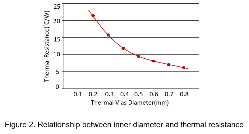
According to the common tendency, the diameter larger , the heat dissipation effect better, but when the diameter is larger than a limit value, the heat dissipation effect may not continue to improve proportionally, and it will also cause incorrect soldering problems during the reflow soldering process, so it need to be extra care required. According to the experimental results in the figure 2, changing the inner diameter affects the thermal resistance. As expected, the larger the inner diameter of the thermal vias, the lower the thermal resistance. In order to optimize the thermal conductivity of the thermal vias, it is recommended to use an inner diameter of about 0.3mm-0.4mm.
2. Distance Between Each Thermal Vias
One of the purposes of the glass fiber board is to increase the support. Once there are too many thermal vias, the external pressure will cause the PCB to tilt easily and the surface will be uneven. From the experimental results, the recommended hole-to-hole spacing is 1.0mm-1.2mm.
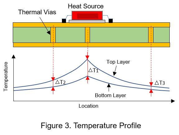
It can be seen from the above that the inner diameter and number of thermal vias have a direct effect on thermal resistance. Further discussing the position of the thermal vias, thermal vias can be placed as close as possible to the heat source, such as directly below or around the heat source, which can speed up the heat dissipation and reduce the thermal resistance. Using the law of heat balance, if the thermal vias are put at a place with a greater temperature difference, the heat-conduction effect will be more significant. It can be seen from Figure 3 that the temperature difference between top layer and bottom layer of thermal vias under heat source is the largest, and the farther away from the heat source, the smaller the temperature difference (ΔT1>ΔT2>ΔT3).
Experiment
In this experiment, the influence of different thermal vias positions on the temperature distribution of the power converter is shown, and then the temperature differences are displayed separately. The specifications of the selected power converter are as follows
| DC to DC Converter | |
| Input voltage | 48 Vdc |
| Output voltage/current | 15 Vdc / 2.7A |
| Operating temperature | -40~105°C |
| Case temperature | Max.110°C |
| Wind speed | 20LFM |
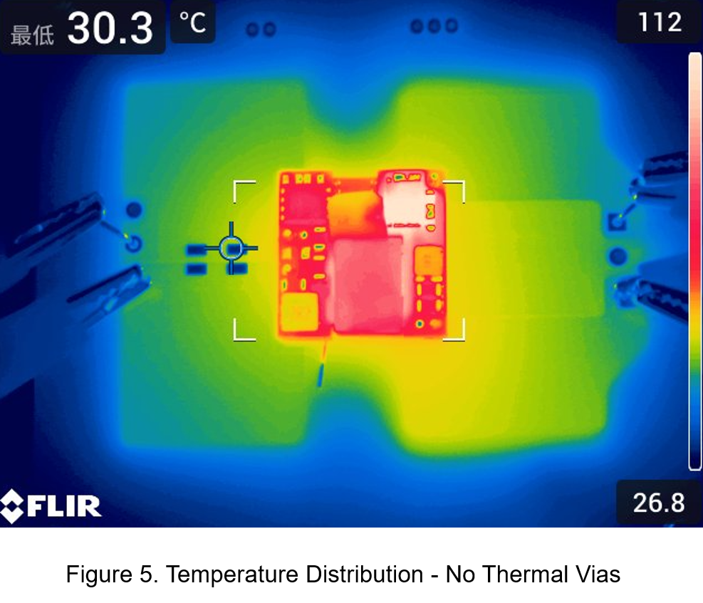
- No Thermal Vias Case
The power converter only uses the shell and the solder joints as the heat dissipation path, so it is obvious that the high temperature area of the PCB is very wide, and the measured temperature is 30.3°C.
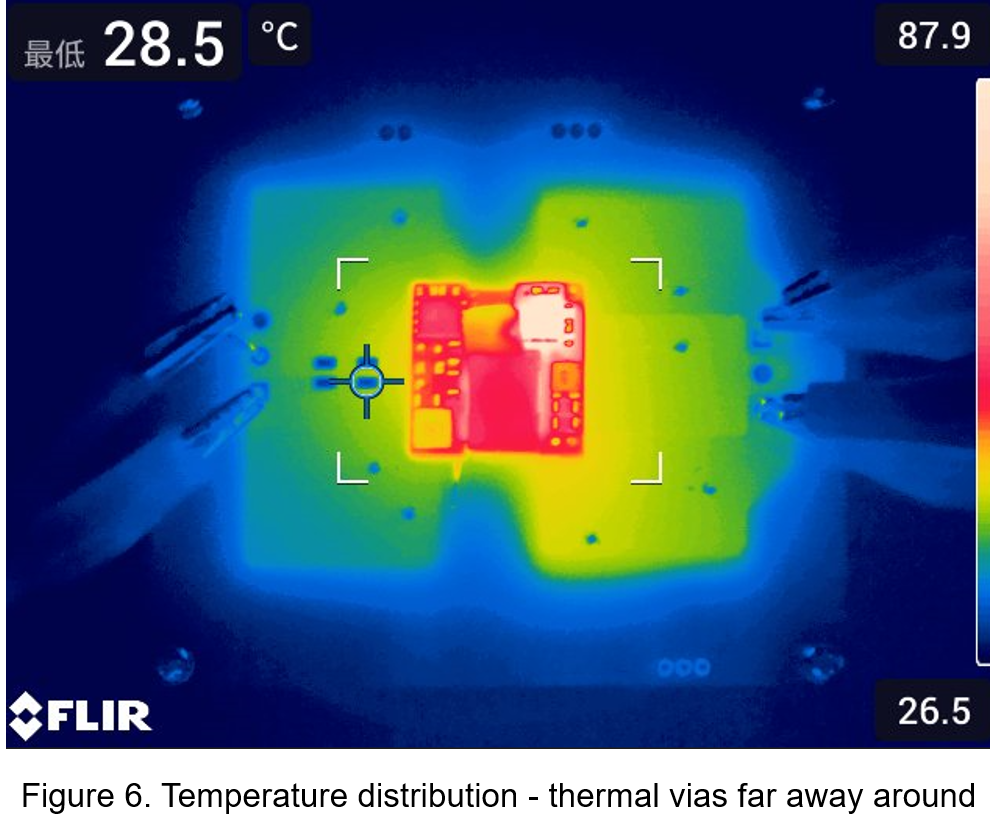
- Thermal Vias Far Away Around Converter
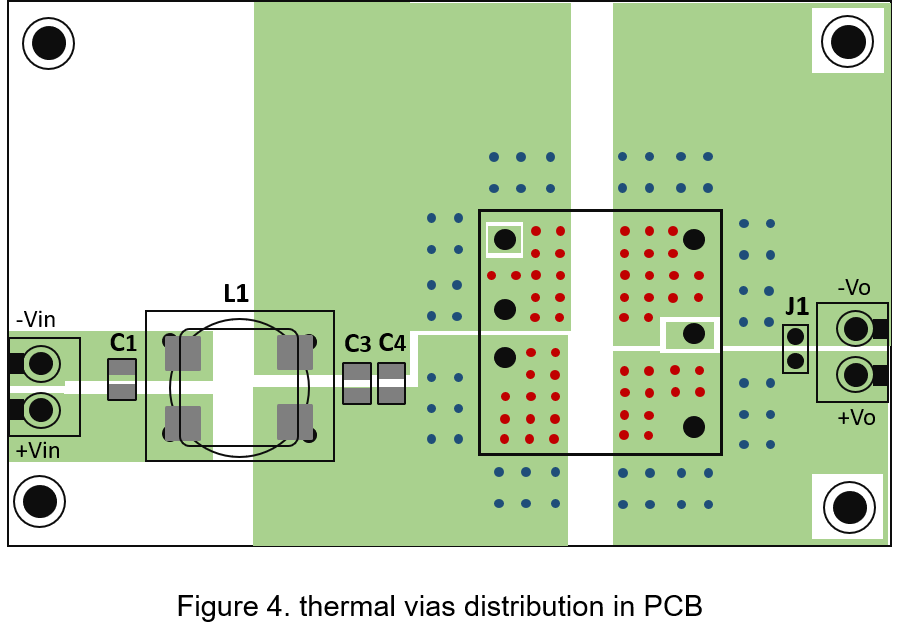
Place the vias (see blue dots in Figure 4) far away the power converter input and output pin,instead of the control logic signal traces, which can reduce the temperature difference pressure. The measurement temperature was 28.5°C. It is about 5.9% lower than no thermal vias case.
- Thermal Vias Near Around Converter
That adds the same number of vias closer to the power converter, and the measured temperature was 22.9°C. The measured temperature is lower about 19.6% than far away vias case.
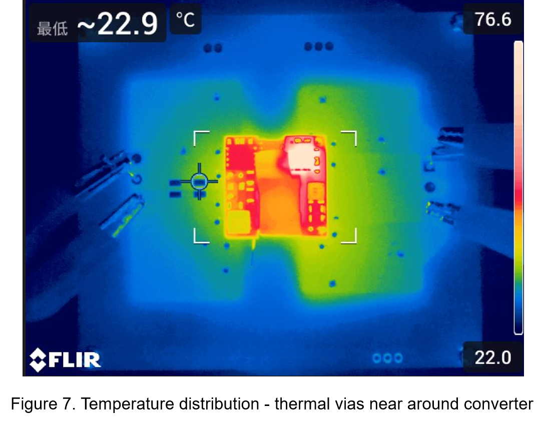
From this experiment, it can be known that through holes closer to the power converter, the better heat dissipation will be.
Conclusion
Many electronic system failures are caused by overheat. There are different ways to transfer the heat away from the PCB. This article explains that following some rules in designing thermal vias can reduce the thermal resistance more effectively, including increasing the number of thermal vias, enlarging the diameter of thermal vias and the position of thermal vias are as close as possible to the heat source. The above solutions can effectively dissipate heat and improve performance and service life of electronic products.
CTC is service provider for high-end power modules (DC to DC Converter and AC to DC Converter) for critical applications worldwide since 1987. We aim to be business generator and a virtual business unit. CTC is your own team with 35 years of experience for a strong business program from market research, product definition & development, supply chain management and total technical services.
CTC is the only corporation certificated with ISO-9001, IATF-16949, ISO22613(IRIS, AFNOR silver certificate), and ESD/ANSI-2020. We can 100% ensure not only the product, but also our workflow and service to match quality management system for every high-end application from the very beginning. From design to manufacturing and technical support, every single detail is operated under highest standard.