

You are here
Back to topConsiderations for Selecting Output Capacitors
An ideal power converter needs to maintain output voltage stability no matter how the load changes. In practical applications, selecting improper output capacitors during load transients will cause excessive ripple voltage and inrush current, thereby affecting the performance of the power converter. This article will introduce the guidelines for selecting output capacitor, detail the effect of load capacitance on the startup process, and provide suggestions for improvement.
Introduction
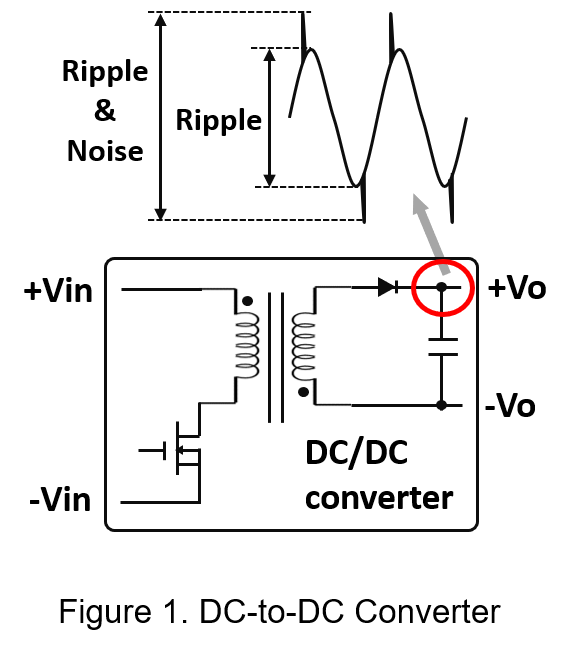
For vehicle battery charging applications, the abnormal output ripple voltage will shorten the battery life, and the large inrush current will cause poor startup and even burn out the input stage circuit. Therefore, how to protect the output voltage and current state is very important to the system. Figure 1 is a schematic diagram of a DC/DC converter. The voltage noise is generated during the MOSFET switching and coupled to the output side through the transformer. And then the ripple measured at the output capacitor is a ripple voltage that contains noise components. The component of ripple voltages content ripple voltage is a lower frequency voltage, and noise voltage is a higher frequency voltage, so when implementing an isolated or non-isolated power converter, many designers choose to add external capacitors are connected to the output of the power converter in parallel, which filters ripple and noise.
Power converters have many topologies, control loops types, and filters to achieve low output ripple voltage and low input inrush current, and even from the design concept, it can improve the output voltage response and reduce filter complexity by increasing the switching frequency.
Output Ripple
First user observes the current flow direction of each node in the power converter, and from figure 3 clearly understands the relationship between the output capacitor and the output ripple voltage during charge and discharge process. The voltage and current waveforms of the step-down power converter operating in the continuous conduction mode shown in the figure 3. Assume each component is an ideal, and the waveforms can help to understand the operation sequence.
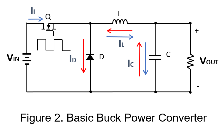

When the power transistor is turned on, the input current flows through the inductor, and the inductor current increases linearly; when the transistor is turned off, the voltage polarity of the inductor is reversed, and the diode becomes forward conduction. Therefore, the energy originally stored in the capacitor is released to the load through the diode and the inductor. It can be seen that the capacitor (
C ) is closely related to the ripple voltage (△V0), and the formula is as follows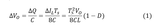
Where△Q is the amount of charge change, Ts is the switching period, D is the duty cycle ratio.
Once in high current application, it must be taken into account non-ideal effects, including equivalent series resistance (ESR) and equivalent series inductance (ESL).
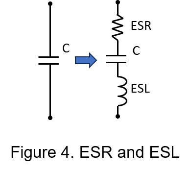
ESR affects the amplitude of the output voltage ripple and is proportional to the load variation. In addition ESR also can exacerbate the output voltage drop. ESL reduces the output capacitor voltage and generates a spike. According to the characteristics of the inductor, the voltage spike generated by ESL is related to the time of load change. If the load rises faster, the voltage spike will be serious, or even out of specification. Change formula (1) to
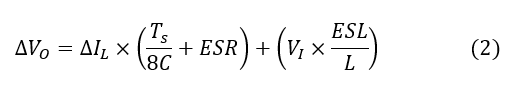
Where V1is the maximum input voltage, △IL is the amount of change in the inductor current.
Parallel output capacitance at power converter is very effective for reducing ripple voltage and improving transient response. Suppose you want to reduce the output ripple voltage and surge voltage, you must reduce ESR and ESL, increase the output capacitance and switching frequency.
Load Capacitance Range
From the previous chapter, we can know that the output terminal of power converter is connected in parallel with an external capacitor in order to reduce ripple and noise
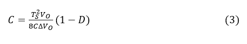
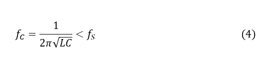
Assuming that the cut-off frequency of the low-pass filter composed of inductors and capacitors is much lower than the operating frequency of the power converter, the output ripple voltage is smaller. According to the user's ripple voltage requirement, the minimum capacitance value can be deduced from formula (3) and (4).
Considering the non-ideal effect of the components, it is recommended to design load capacitance value to be at least ten times larger than the calculated value to get better performance.
For the requirement of reducing the output ripple, many users will choose an excessively large load capacitance. With the increase of the load capacitance gradually, the over inrush current will cause the power converter to delay startup time or even fail to work. The reason is that when the initial input voltage is started, the output capacitor has no charge, so the output terminal during this period is regarded as a short circuit, which causes the input surge current to be too large instantaneously, resulting in a longer start-up time.

For large load capacitances, inrush current peaks can trigger the power converter overcurrent protection circuit, shutting down the power converter temporarily, and then attempting to restart autonomously, whereas if the cycle of continuous shutdown and startup occurs continuously, the power converter maybe suffer permanent damage.
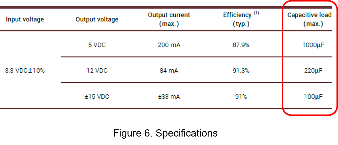
Therefore, that is important to choose the maximum value of the load capacitance while maintaining startup performance. As shown in the figure, the maximum load capacitance value is clearly marked on the specification sheet. Once the selected capacitance is higher than this value, it is likely to meet poor startup problems.
Experiment
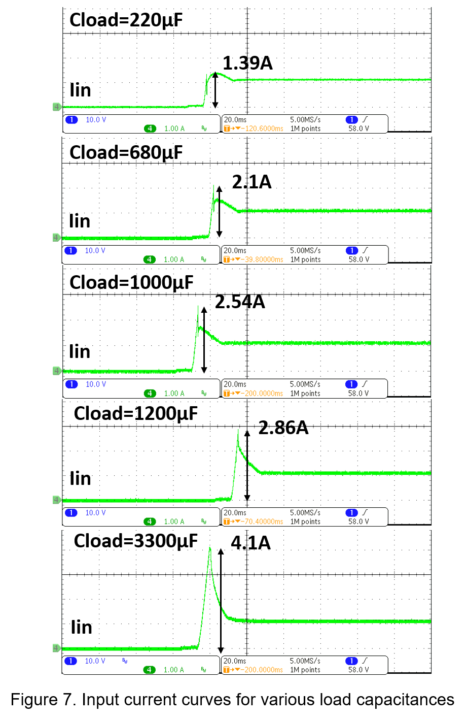
In the following, a specific DC-to-DC converter will be used to measure the difference in input current by current probe before and after through different output capacitors. The converter is a wide input voltage range from 9 to 36V input, 12V output regulated converter, the output power is 30W, the output current is 2.5A, the specifications are shown in Table 1.
| DC to DC Converter | |
| Input voltage | 24 Vdc |
| Typ. output voltage | 12 Vdc |
| Output current @full load | 2.5A |
| Input current @no load | 10mA |
| Max. capacitive load | 1200µF |
Figures 7 shows the input current waveforms using 220µF, 680µF, 820µF, 1200µF, and 3300µF of load capacitors. It can be seen that the larger the capacitive load, the higher the inrush current. When using the maximum load capacitance, the inrush current has reached 2.86A, which is greater than the maximum load current.
Conclusion
Selecting the correct load capacitor is very important for the power converter. In order to reduce the ripple voltage and noise, it is effective to choose load capacitor with low ESR and ESL. However, if the load capacitor continues to increase, it will also cause poor startup. Hence, limiting the increase in output capacitance allows a good balance between filtering and inrush current.
CTC is service provider for high-end power modules (DC to DC Converter and AC to DC Converter) for critical applications worldwide since 1987. We aim to be business generator and a virtual business unit. CTC is your own team with 35 years of experience for a strong business program from market research, product definition & development, supply chain management and total technical services.
CTC is the only corporation certificated with ISO-9001, IATF-16949, ISO22613(IRIS, AFNOR silver certificate), and ESD/ANSI-2020. We can 100% ensure not only the product, but also our workflow and service to match quality management system for every high-end application from the very beginning. From design to manufacturing and technical support, every single detail is operated under highest standard.