You are here
Back to topGeneral Layout Guidance for DC-DC Converter
Proper layout and parts placement are very important for converter, because it will help to give full play to the capabilities of the converter. Improper layout may increase output voltage ripple, or higher EMI noise, or insufficient heat dissipation of the converter, resulting in abnormal temperature rise. The above-mentioned problems can be solved by appropriate layout method. This paper provides several layout methods for reference as below.
1. Current Path
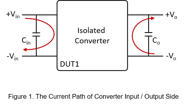
Figure 1 shows the current path of the converter in red line. The purpose of adding input and output capacitors (Cin, Co) are reduce the input current and output voltage ripple. Below has some note for layout.
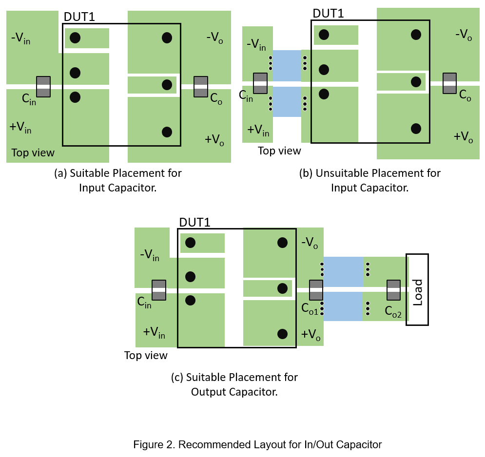
- Place the Cin and Co close to the converter as Figure 2(a) shows.
- Figure 2(b) shows that the input capacitor is far away from the converter or cannot be place on the same layer. This may increase input current ripple, causing high output ripple noise or unstable the converter.
If the layout path has long distance between converter and load point as Figure 2(c) shows. It is recommended to connect capacitors at both ends to reduce the output voltage ripple.
2. PCB Layout and the Trace
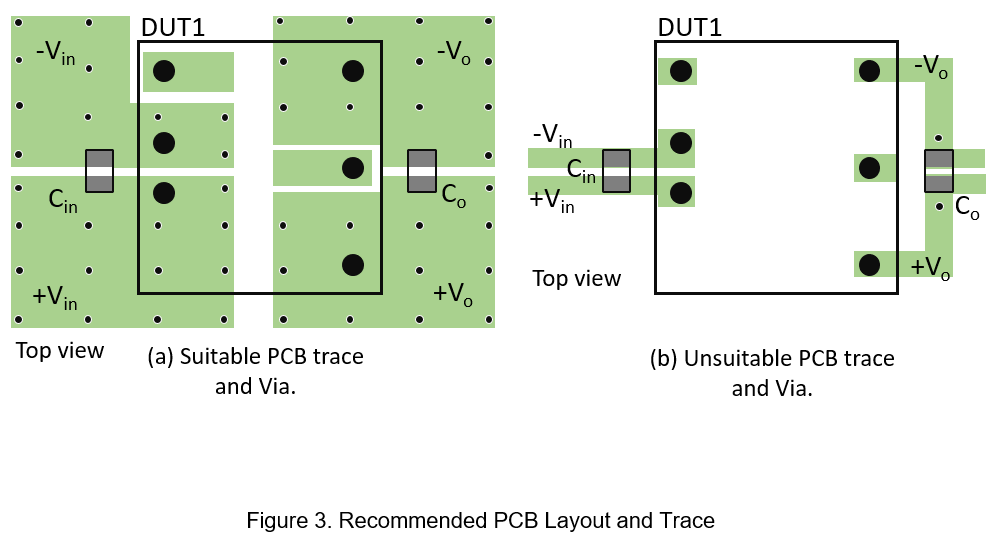
Proper copper area helps the converter to dissipate heat through the pins. However, in practical applications, it is hard to achieve sufficient heat dissipation PCB area on single layer. So, the common method is through multilayer board to increase the PCB area, and use through-hole to connected.
Through-holes can help conduct the heat to other PCB layers, Figure 3(a) is the suitable layout. For insufficient PCB layout or trace, as shown in Figure 3(b). The converter can not dissipation the heat to PCB, so the converter will operated at high temperature states, which might cause damage for the converter.
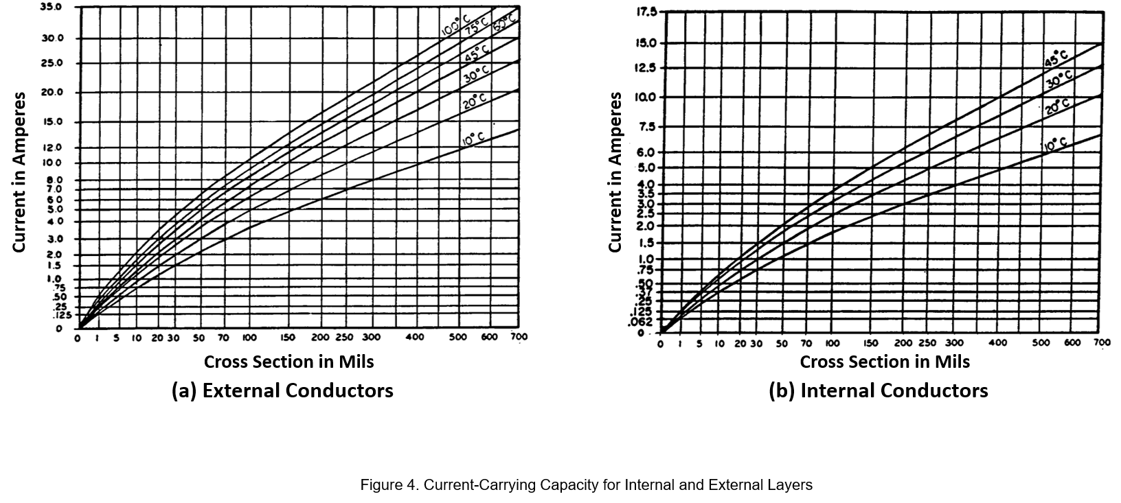
The current-carrying capacity of the PCB can be divided into internal and external part. And the maximum current-carrying capacity of the internal circuit is set to half of the external circuit. Figure 4 is the current-carrying chart of the external and internal circuits, which shown in IPC-2111 section 6.2.
In addition, it can used below formula to calculate the PCB layout trace.
![]()
K: Correction factor, internal: 0.024; external: 0.048.
△T: Temperature rise of PCB (°C)
A: PCB cross-sectional area (mil2)
I: Maximum current-carrying capacity (A)
Assuming that the current is 1A, the thickness of the PCB is 1oz/ft2, and the temperature rise is 10°C. The result is, for internal layer, it needed 30.8mil. And for external layer, it needed 11.8mil.
As refer to the Figure 4. Under same condition, the external layer need 17mil. And the internal layer need 44mil. It is recommended to use a wider value here.
3. The Placement for EMI Parts
EMI is divided into conducted and radiated noise. Conducted noise refers to noise conducted through wires or PCB trace. Radiated noise refers to the noise emitted (radiated) to area. Each application had relative EMI requirements. Such as EN55011 (CISPR11) used in industry or medical application, and EN55032 (CISPR32) commonly used in the ICT application. Marine needed to comply with EN60945.
The datasheet of converter will show the external circuit for EMI. PI-filter, Common-Mode Choke and Safety capacitor are the most common method for solving EMI. It is very important to choose the right parts. In addition, the placement and layout often affect the EMI results. The following will show some layout methods for EMI external circuit.
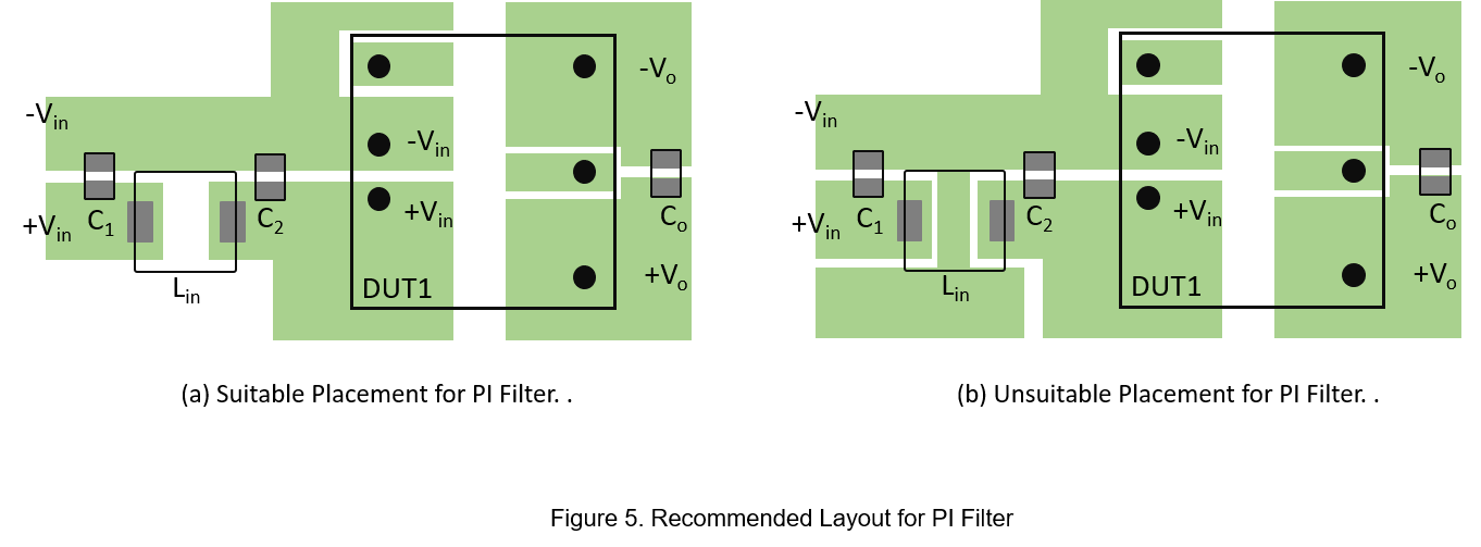
- PI Filter
The PI filter is one of the common external circuit for EMI, which is composed of inductors and capacitors. The recommended layout is shown in Figure 5(a). In order to avoid unnecessary noise interference. As Figure 5(b) shows, do not wiring directly under the inductor.
- Common Mode Choke Filter
When the common mode current (ICM) flows in, the ICM are in the same direction. The magnetic flux is enhanced, and the inductance of the common mode inductor is increased, so that the common mode current is suppressed. When the differential mode current (IDM) flows in, the common mode currents on both sides are in opposite directions, the magnetic flux is cancelled, and the IDM passes directly.
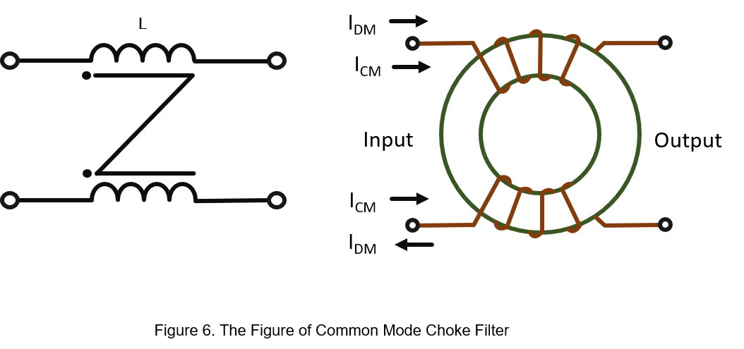
Figure 7(a) shows the recommended PCB layout for CMC filter. Do not wiring directly under the CMC filter, as shown in Figure 7(b). Do not cross the output side of the CMC filter, or the input and output are too close to avoid reducing the suppression capability, as shown in Figure 7(c).

- Safety Capacitor
Safety capacitor means it will not cause electric shock after the capacitor failure. And it includes X and Y capacitor. The X capacitor is connected across the two lines of the power line. The X capacitor can suppress differential mode interference and often used in AC-to-DC converter applications.
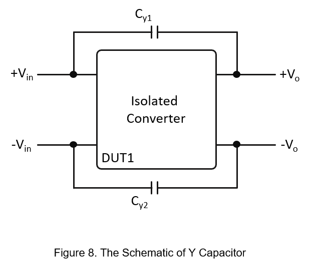
The Y capacitor can suppress common mode interference and is usually connected across the primary and secondary of the converter. The purpose is to provide a current loop for the secondary common-mode current to the primary side, reducing the impact of the common-mode current on the output side, as shown in Figure 8.
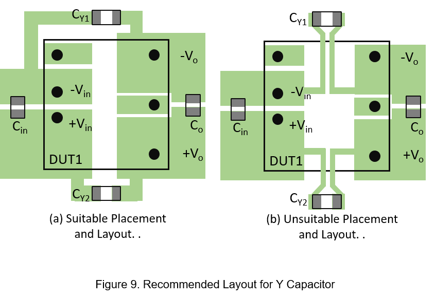
Figure 9(a) shows the recommended layout of Y capacitors. It needed to confirm the isolation voltage of the capacitor is higher than the actual application. Or, it will damage the Y capacitors. So, if the isolation voltage requirement is high, the primary and secondary trace should not be too close, such as Figure 9(b). And, if the converter case is metal, the Y capacitor should not be too close to the converter to avoid insufficient isolation distance.
- The Layout Tips for Brick Type DC/DC Converter
The most difference of general converter and brick-type converter is the brick-type has aluminum base-plate.
So, the solution for EMI is slightly different from general ones.
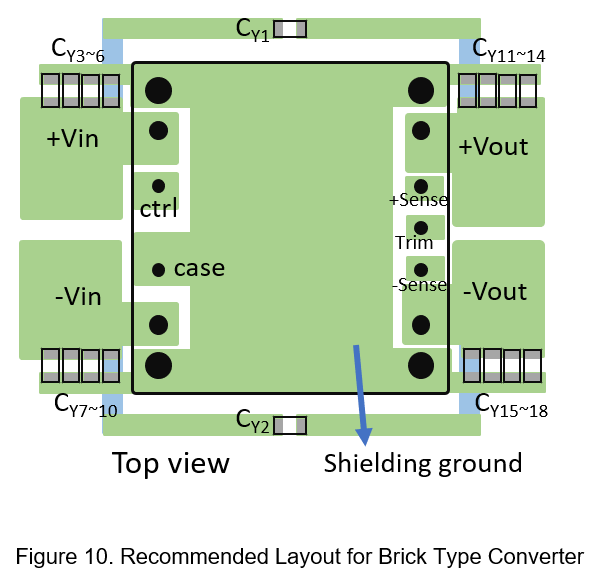
- On the same layer of the converter, reserve PCB area of the same size as the converter and connect it to the base-plate screw hole. As shown in Figure 10.
- It is not recommended to connect the base-plate to the system ground. Unless there is a description in the product datasheet.
- For better operating temperature, the aluminum base-plate can be connected to the system housing through an isolated thermal pad.
- The input and output pin are connected to the Y capacitors of the aluminum base-plate for better EMI performance.
- Please connect Y capacitors to the input or output pins as close as possible, as shown in Figure 10.
Conclusion
Appropriate layout can help to improve the performance of the converter. But each design has its own requirements. So, it is hard to standardized the layout rule. This paper introduces methods that have been found useful. And provide some suitable and unsuitable layout methods, and user can adjust their own design from it.
CTC is a professional service provider for high-end power supply modules (AC to DC Converter and DC to DC Converter) for critical applications worldwide since 30 years. Our core competence is to design and deliver products with leading technologies, competitive pricing, extremely flexible lead-time, global technical service and high-quality manufacturing (Made In Taiwan).
CTC is the only corporation certificated with ISO-9001, IATF-16949, ISO22613(IRIS), and ESD/ANSI-2020. We can 100% ensure not only the product, but also our workflow and service to match quality management system for every high-end application from the very beginning. From design to manufacturing and technical support, every single detail is operated under highest standard.

